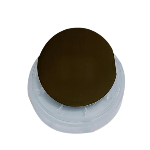
GaAs Substrate


Gallium arsenide substrates are mainly used for circuit substrates, infrared detectors, gamma photon detectors, etc. Because its electron mobility is 5-6 times larger than silicon, it has been importantly used in the manufacture of microwave devices and high-speed digital circuits.
Fuleda can provide 2~8 inches high purity gallium nitride substrate.
| Growth Method | VGF | ||
| Type | S-C-N | ||
| Diameter | 100±0.25mm | ||
| Dopant | GaAs-Si | ||
| Orientation | (100)15°士0.5° off toward | ||
| OF location/length | EJ [ 0-1-1]土0.5°/32.5±1 | ||
| Ingot CC | Min: 0.7E18/cm3 | Max: 3.2E18/cm3 | |
| Resistivity | Min: 1.2E-3 Ω·cm | Max: 8.9E-3 Ω·cm | |
| Mobility | Min: 1628 cm2/v.s | Max: 2642 cm2/v.s | |
| EPD | Max: 5000 / cm2 | ||
| Edge Rounding | 0.25 mmR | ||
| Thickness | 350±25 μm | ||
| TTV/TIR | Max: 10 μm | ||
| BOW | Max: 10 μm | ||
| Warp | Max: 10 μm | ||
| Surface Finish- front | Polished | ||
| Surface Finish -back | Etched | ||
| Partical Count | <50 (size> 0.3μm,Count/wafer) | ||
| Epi-Ready | Yes | ||